The channel resistance of an $\text{N}$-channel $\text{JFET}$ shown in the figure below is $600 \; \Omega$ when the full channel thickness $\left(\mathrm{t}_{\mathrm{ch}}\right)$ of $10 \; \mu \mathrm{m}$ is available for conduction. The built-in voltage of the gate $\mathrm{P}^{+} \; \mathrm{N}$ junction $\left(\mathrm{V}_{\mathrm{b} i}\right)$ is $-1 \mathrm{~V}$. When the gate to source voltage $\left(\mathrm{V}_{\mathrm{GS}}\right)$ is $0 \mathrm{~V}$, the channel is depleted by $1 \; \mu \mathrm{m}$ on each side due to the built-in voltage and hence the thickness available for conduction is only $8 \; \mu \mathrm{m}$.
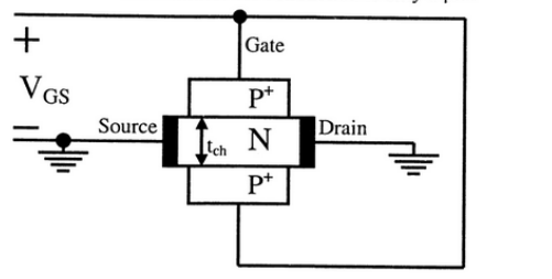
The channel resistance when $\mathrm{V}_{\mathrm{GS}}=-3 \mathrm{~V}$ is
- $360 \; \Omega$
- $917 \; \Omega$
- $1000 \; \Omega$
- $3000 \; \Omega$