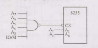
An $8255$ chip is interfaced to an $8085$ microprocessor system as an $\mathrm{I} / \mathrm{O}$ mapped $\mathrm{I} / \mathrm{O}$ as shown in the figure. The address lines $\mathrm{A}_{0}$ and $\mathrm{A}_{1}$ of the $8085$ are used by the $8255$ chip to decode internally its three ports and the Control register. The address lines $A_{3}$ to $\mathrm{A}_{7}$ as well as the $I O / \overline{M}$ signal are used for address decoding. The range of addresses for which the $8255$ chip would get selected is
- $\mathrm{F} 8 \mathrm{H}-\mathrm{FBH}$
- $\mathrm{F} 8 \mathrm{H}-\mathrm{FCH}$
- $\mathrm{F} 8 \mathrm{H}-\mathrm{FFH}$
- $\mathrm{F0H}-\mathrm{F} 7 \mathrm{H}$