The circuit diagram of a standard $\text{TTL NOT}$ gate is shown in the figure. When $V_{i}=2.5 \mathrm{~V},$ the modes of operation of the transistors will be
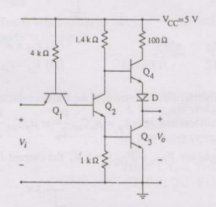
- $\mathrm{Q}_{1}$ : reverse active; $\mathrm{Q}_{2}$ : normal active; $\mathrm{Q}_{3}$ : saturation; $\mathrm{Q}_{4}$ : cut-off
- $\mathrm{Q}_{1}$ : reverse active; $\mathrm{Q}_{2}$ : saturation; $\mathrm{Q}_{3}$ : saturation; $\mathrm{Q}_{4}$ : cut-off
- $\mathrm{Q}_{1}$ : normal active; $\mathrm{Q}_{2}$ : cut-off; $\quad \mathrm{Q}_{3}$ : cut-off; $\quad \mathrm{Q}_{4}$ : saturation
- $\mathrm{Q}_{1}$ : saturation; $\quad \mathrm{Q}_{2}$ : saturation; $\quad \mathrm{Q}_{3}$ : saturation; $\mathrm{Q}_{4}$ : normal active