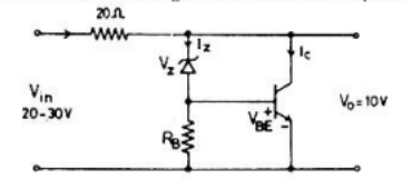
The transistor shunt regulator shown in the figure is has a regulated output voltage of $10 \mathrm{~V}$, when the input varies from $20 \mathrm{~V}$ to $30 \mathrm{~V}$. The relevant parameters for the zener diode and the transistor are: $\mathrm{V}_{\text{Z}}=9.5, \mathrm{~V}_{\text {SE }}=0.3 \mathrm{~V}, \beta=99$. Neglect the current through $R_{B}$. Then the maximum power dissipated in the zener diode $(\mathrm{P}_{\mathrm{Z}})$ and the transistor $(\mathrm{P}_{\mathrm{T}})$ are
- $\mathrm{P}_{\mathrm{Z}}=75 \mathrm{~mW}, \mathrm{P}_{\mathrm{T}}=7.9 \mathrm{~W}$
- $\mathrm{P}_{\mathrm{Z}}=85 \mathrm{~mW}, \mathrm{P}_{\mathrm{T}} = 8.9 \mathrm{~W}$
- $\mathrm{P}_{\mathrm{Z}}=95 \mathrm{~mW}, \mathrm{P}_{\mathrm{T}}=9.9 \mathrm{~W}$
- $\mathrm{P}_{\mathrm{Z}}=115 \mathrm{~mW}, \mathrm{P}_{\mathrm{T}}=11.9 \mathrm{~W}$