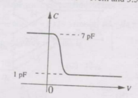
The figure shows the high-frequency capacitance-voltage (C-V) characteristics of a $\mathrm{Metal} / \mathrm{SiO}_{2} / \text{silicon (MOS)}$ capacitor having an area of $1 \times 10^{-4} \mathrm{~cm}^{2}$. Assume that the permittivities $\left(\varepsilon_{0} \varepsilon_{r}\right)$ of silicon and $\mathrm{SiO}_{2}$ are $1 \times 10^{-12} \mathrm{~F/cm}$ and $3.5 \times 10^{-13} \mathrm{~F/cm}$ respectively.
The maximum depletion layer width in silicon is
- $0.143 \; \mu \mathrm{m}$
- $0.857 \; \mu \mathrm{m}$
- $1 \; \mu \mathrm{m}$
- $1.143 \; \mu \mathrm{m}$