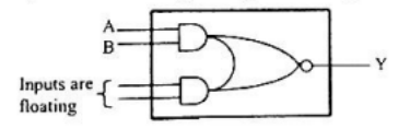
0 votes 0 votes Figure given below shows the internal schematic of a $\text{TTL AND-OR}$ -Invert $\text{(AOI)}$ gate. For the inputs shown in the given figure, the output $\text{Y}$ is $0$ $1$ $\mathrm{AB}$ $\overline{\mathrm{AB}}$ Others gate2004-ec + – admin asked Sep 25, 2022 • edited Nov 30, 2023 by makhdoom ghaya admin 46.4k points 141 views answer comment Share Follow See all 0 reply Please log in or register to add a comment.