In the circuit shown in the figure $\mathrm{A}$ is a parallel-in, parallel-out $4$ bit register, which loads at the rising edge of the clock $C$. The input lines are connected to a $4$ bit bus, $W.$ Its output acts as the input to a $16 \times 4$ ROM whose output is floating when the enable input $E$ is $0.$ A partial table of the contents of the ROM is as follows
$$\begin{array}{|l|c|c|c|c|c|c|c|c|}
\hline \text{Address} & 0 & 2 & 4 & 6 & 8 & 10 & 11 & 14 \\
\hline \text{Data} & 0011 & 1111 & 0100 & 1010 & 1011 & 1000 & 0010 & 1000 \\
\hline\end{array}$$
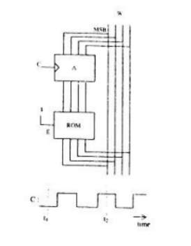
The clock to the register is shown, and the data on the $W$ bus at time $t_{1}$ is $0110.$ The data on the bus at time $t_{2}$ is
- $1111$
- $1011$
- $1000$
- $0010$