retagged by
448 views
0 0 votes

In the figure, $D1$ is a real silicon $pn$ junction diode with a drop of $0.7V$ under forward bias condition and $D2$ is a Zener diode breakdown voltage of $-6.8V$. The input $V_{in}(t)$ is a periodic square wave of period $T$, whose one period is shown in the figure.
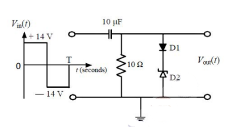
Assuming $10 \tau < < T$, where $\tau$ is the time constant of the circuit, the maximum and minimum values of the output waveform are respectively,

  1. $7.5 V$ and $-20.5 V$
  2. $6.1 V$ and $-21.9 V$
  3. $7.5 V$ and $-21.2 V$
  4. $6.1 V$ and $-22.6 V$

Please log in or register to answer this question.

Answer:
Position:
Show:

Related questions

0 0 votes
0 0 answers
496
496 views
admin asked Nov 25, 2017
496 views
An electron $(q_1)$ is moving in free space with velocity $10^5$ m/s towards a stationary electron $(q_2)$ far away. The closest distance that this moving electron gets t...
0 0 votes
0 0 answers
620
620 views
admin asked Nov 25, 2017
620 views
A MOS capacitor is fabricated on $p$-type Si (Silicon) where the metal work function is $4.1$ eV and electron affinity of Si is $4.0$ eV. $E_C-E_F=0.9$ eV, where $E_C$ an...
0 0 votes
0 0 answers
356
356 views
admin asked Nov 23, 2017
356 views
Consider an $n$-channel MOSFET having width $W$, length $L$, electron mobility in the channel $\mu _{n}$ and oxide capacitance per unit area $C_{ox}$. If gate-to-source $...
0 0 votes
0 0 answers
646
646 views
admin asked Nov 25, 2017
646 views
An abrupt $pn$ junction (located at $x=0$) is uniformly doped on both $p$ and $n$ sides. The width of the depletion region is $W$ and the electric field variation in the ...

Add Synced Question

×