• recategorized by
511 views
0 0 votes

For the transistor $M_{1}$ in the circuit shown in the figure, $\mu_{n} C_{\text{ox}} = 100\:\mu A/V^{2}$ and $(W/L)=10$, where $\mu_{n}$ is the mobility of electron, $C_{\text{ox}}$ is the oxide capacitance per unit area , $W$ is the width and $L$ is the length.
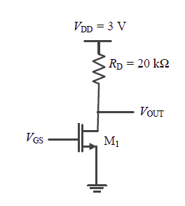
The channel length modulation coefficient is ignored. If the gate-to-source voltage $V_{\text{GS}}$ is $1\:V$ to keep the transistor at the edge of saturation, then the threshold voltage of the transistor (rounded off to one decimal place) is __________________ $V$.

Please log in or register to answer this question.

Answer:
Position:
Show:

Related questions

0 0 votes
0 0 answers
811
811 views
Arjun asked Feb 19, 2021
811 views
​​​​​​​In the circuit shown in the figure, the transistors $M_{1}$ and $M_{2}$ are operating in saturation. The channel length modulation coefficients of both the transis...
0 0 votes
0 0 answers
571
571 views
Arjun asked Feb 19, 2021
571 views
A silicon $P-N$ junction is shown in the figure. The doping in the $P$ region is $5\times10^{16}\:cm^{-3}$ and doping in the $N$ region is $10\times10^{16}\:cm^{-3}$. The...
0 0 votes
0 0 answers
511
511 views
Arjun asked Feb 19, 2021
511 views
Consider a polar non-return to zero ($\text{NRZ}$) waveform, using $+2\:V$ and $-2\:V$ for representing binary ‘$1$’ and ‘$0$’ respectively, is transmitted in the presenc...
0 0 votes
0 0 answers
489
489 views
Arjun asked Feb 19, 2021
489 views
For an $n$-channel silicon $\text{MOSFET}$ with $10\:nm$ gate oxide thickness, the substrate sensitivity $\left ( \partial V_{T}/\partial \left | V_{BS} \right | \right )...

Add Synced Question

×