The transistor in the circuit shown in the figure is so biased ($dc$ biasing network is not shown) that the $dc$ collecter current $I_{c}=1 \mathrm{~mA}$. Supply is $V_{cc}=5 \mathrm{~V}$.
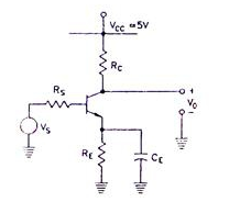
The network components have following values
\[\begin{array}{l} R_{c}=2 k \Omega, \\ R_{s}=1.4 k \Omega \\ R_{E}=100 \Omega \end{array}\]
and
The transistor has specifications.
$\beta=100$ and base spreading resistance
\[r_{b b}=100 \; \Omega .\]
Assume $\frac{k T}{q}=25 \; \mathrm{mV}$
Evaluate small signal Voltage Gain $\mathrm{A}_{\mathrm{V}_{\mathrm{s}}}$ at a frequency of $10 \; \mathrm{kHz}$, and Input Resistance $\mathrm{R}_{i}$ for two cases
- $\text{CE}$, the hypass capacitor across $R_{E}$ is $25 \mu \mathrm{F}$.
- The bypass capacitor $C_{E}$ is removed leaving $R_{E}$ unbypassed